
As electronic assemblies become smaller and more densely populated, conventional optical inspection has limitations when defects are located beneath components or inside packages. Hidden solder joints, voids, internal cracks, and structural abnormalities cannot always be identified from the surface.
For electronics manufacturers, EMS providers, semiconductor companies, and industrial production facilities, X-ray inspection provides a non-destructive method for examining internal structures. A properly configured PCB inspection machine can therefore become an important part of process quality control, particularly when combined with automated optical inspection and other inspection technologies.
Seamark ZM develops microfocus X-ray inspection equipment for electronics and industrial applications. Its solutions are designed around high-resolution imaging, flexible inspection configurations, and automated analysis for manufacturers that require more than conventional visual inspection.
AOI systems and X-ray systems solve different inspection problems.
AOI inspection equipment uses cameras and optical algorithms to inspect visible surfaces. It is highly effective for detecting issues such as component presence, polarity, solder appearance, placement errors, and other surface-level defects.
An X-ray system, by contrast, penetrates the assembly and produces images of internal structures. This makes PCB X-ray inspection particularly valuable when solder joints or components are hidden.
Typical applications include:
BGA solder-joint inspection
QFN and other bottom-terminated packages
Voids in solder joints
Internal component defects
Through-hole solder inspection
PCB assembly quality verification
Semiconductor package inspection
Failure analysis and process development
For this reason, an X-ray system should not necessarily be considered an alternative to an AOI inspection machine. In many production environments, AOI and X-ray are complementary technologies.
When manufacturers search for a PCB machine for sale, price alone should not determine the purchasing decision. The equipment needs to match the physical and technical characteristics of the assemblies being inspected.
Important parameters include X-ray source voltage, tube current, focal spot size, detector resolution, imaging area, sample dimensions, sample weight, magnification, and software capability.
A microfocus source is especially important for high-resolution electronics inspection. A smaller focal spot can improve image sharpness and help manufacturers identify small internal defects.
The inspection area is another consideration. A compact system may be sufficient for mobile-device PCBs or laboratory applications, while automotive control units, server boards, and industrial assemblies may require a larger working area.
Manufacturers should also determine whether they need 2D inspection, oblique imaging, laminography, or 3D/CT capabilities. The appropriate configuration depends on the type of defect being investigated and the complexity of the assembly.
Microfocus technology is particularly relevant to electronics manufacturing because PCB assemblies can contain very small structures.
A conventional X-ray source may not provide sufficient spatial resolution for certain fine-pitch components. A microfocus source reduces the effective focal spot and can improve the ability to distinguish closely positioned structures.
Seamark ZM's microfocus X-ray inspection machines are designed for applications where high-resolution internal imaging is required. Depending on the configuration, the equipment can be used for PCBAs, semiconductor components, electronic devices, and other industrial inspection applications.
For engineering teams, this capability is particularly useful during process development and failure analysis, where the objective is not simply to determine whether a product passes or fails but to understand why a defect occurred.
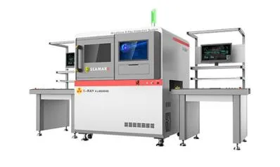
SMT X-ray inspection becomes increasingly important as surface-mount packages become more compact.
Modern SMT assemblies frequently use BGA, CSP, QFN, DFN, and other packages in which critical solder connections are partially or completely hidden. Optical systems may identify external symptoms, but X-ray imaging can directly examine the internal solder structure.
In a production environment, X-ray inspection can be positioned at different stages depending on the manufacturer's quality strategy:
Incoming component verification → SMT assembly → AOI → X-ray inspection → functional testing → final quality control
Not every board needs to undergo the same inspection depth. Manufacturers may apply sampling inspection, risk-based inspection, or 100% inspection depending on product value, customer requirements, failure consequences, and production volume.
For high-reliability products, X-ray data can also provide process feedback. For example, recurring solder voids may indicate problems involving stencil design, solder paste, reflow temperature profiles, component geometry, or PCB thermal characteristics.
One of the most established applications of PCB X-ray inspection is BGA analysis.
BGA packages place solder balls underneath the component, making direct visual examination difficult after assembly. X-ray imaging can reveal solder-ball geometry and identify abnormalities that would otherwise remain hidden.
A dedicated BGA inspection system may be used to evaluate:
Solder bridging
Missing solder connections
Excess solder
Insufficient solder
Voids
Misalignment
Irregular solder-ball formation
The inspection objective should determine the required imaging angle, resolution, and software functions. For high-volume production, automated defect recognition can reduce dependence on manual image interpretation.
Manufacturers sometimes compare automated optical inspection equipment with X-ray inspection as though one technology must replace the other.
In practice, they address different defect categories.
AOI is fast and efficient for surface inspection. It can inspect component placement, markings, solder appearance, polarity, and other visible characteristics.
X-ray inspection examines internal structures and is therefore better suited to hidden solder joints, internal voids, and package-level defects.
A production line may consequently use an AOI inspection machine for rapid screening and X-ray inspection for selected boards or critical components.
The combination can provide broader defect coverage without requiring every inspection technology to perform every task.
As semiconductor packages become smaller and more complex, inspection requirements become more demanding.
Semiconductor inspection equipment may need to identify internal package defects, bonding abnormalities, voids, cracks, delamination, or other structural problems without damaging the device.
X-ray inspection is valuable because it is nondestructive and can examine internal structures that cannot be accessed through ordinary optical methods.
For semiconductor packaging and advanced electronics, manufacturers should pay particular attention to focal spot size, detector performance, geometric magnification, image processing, and repeatability.
For R&D and failure-analysis laboratories, the ability to change viewing angles and magnification can be as important as automated production speed.
Beyond PCB assemblies, X-ray inspection is used across industrial manufacturing.
Industrial automated X-ray inspection solutions can support inspection of castings, electronic modules, batteries, connectors, and other components where internal quality cannot be confirmed visually.
Automation becomes particularly valuable when manufacturers need consistent inspection criteria across large production volumes. Software can assist with image acquisition, defect recognition, classification, storage, and reporting.
However, automation should not be evaluated solely on throughput. Manufacturers should also examine false-positive and false-negative performance, recipe management, data traceability, integration with MES or factory systems, and the ability to adapt inspection parameters to different products.
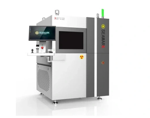
When comparing an inspection machine for sale, B2B buyers should create a technical specification based on actual production samples.
A practical evaluation should include:
1. Sample compatibility – PCB dimensions, component height, weight, and material.
2. Resolution requirements – smallest defect or structure that must be identified.
3. Inspection method – 2D, angled 2D, laminography, or CT.
4. Throughput – required cycle time and daily production volume.
5. Automation – manual loading versus automated handling.
6. Software – defect recognition, image processing, reporting, and recipe management.
7. Connectivity – MES, ERP, or factory data integration.
8. Safety – shielding, interlocks, warning systems, and radiation protection.
9. Serviceability – calibration, preventive maintenance, spare parts, and technical support.
Testing the actual PCB samples before purchase is particularly important. A machine that performs well on a demonstration sample may not necessarily deliver the same results on a customer's specific assembly.
Because X-ray inspection equipment generates ionizing radiation, safety and regulatory compliance are critical purchasing considerations.
A manufacturing facility should evaluate the system's shielding design, safety interlocks, emergency controls, warning indicators, operating procedures, and applicable national regulations.
Compliance requirements vary by country and installation environment. Therefore, manufacturers should confirm the exact certifications supplied with the selected Seamark ZM configuration and determine whether additional local registration, inspection, operator training, or radiation-safety procedures are required.
For quality systems, inspection records should also be controlled. Storing X-ray images, inspection results, product identifiers, and process parameters can improve traceability and support failure analysis.
The best inspection system is not necessarily the most powerful or expensive machine. It is the system that provides the required defect visibility at the required production speed while remaining practical to operate and maintain.
For electronics manufacturers, the decision should begin with the defects that need to be detected. AOI may provide efficient surface inspection, while X-ray addresses hidden structures. Microfocus X-ray equipment becomes particularly valuable when small features require high-resolution imaging.
Seamark ZM's microfocus X-ray inspection solutions provide a platform for manufacturers evaluating PCBA, semiconductor, and industrial inspection applications. By matching X-ray source performance, detector technology, automation, software, and safety features to the actual production requirement, manufacturers can build a more reliable and measurable inspection process.
PCB X-ray inspection is a nondestructive inspection method that uses X-rays to visualize internal structures of printed circuit boards and assemblies. It is commonly used to examine hidden solder joints, component connections, and internal defects.
Neither technology is universally better. AOI is generally more suitable for fast inspection of visible surfaces, while X-ray is more suitable for internal structures and hidden solder joints. Many electronics manufacturers use both.
Depending on the system and application, X-ray can help identify solder voids, bridges, insufficient solder, open connections, component abnormalities, and other internal structural defects.
A microfocus X-ray machine uses an X-ray source with a very small focal spot to provide high-resolution imaging. This is particularly useful for inspecting small electronic components and fine structures.
X-ray inspection is a nondestructive testing method and does not require the PCB to be physically opened. However, the equipment itself produces ionizing radiation, so appropriate shielding and safety controls are essential.
Manufacturers should evaluate X-ray source specifications, focal spot size, detector resolution, sample dimensions, inspection speed, automation, software, data integration, maintenance, radiation safety, certifications, and after-sales support.
Yes. X-ray technology can be used to inspect internal structures in semiconductor packages and electronic devices. The required resolution and imaging method depend on package design and the defects being investigated.
 EN
EN
 es
es  ko
ko  de
de  it
it  pt
pt  th
th  ar
ar  pl
pl  vi
vi  tr
tr  ru
ru